‘Like a field plowed prior to planting’: Researchers want to grow lasers, yes lasers, on material commonly found in sand
Posted by:
John Harrison
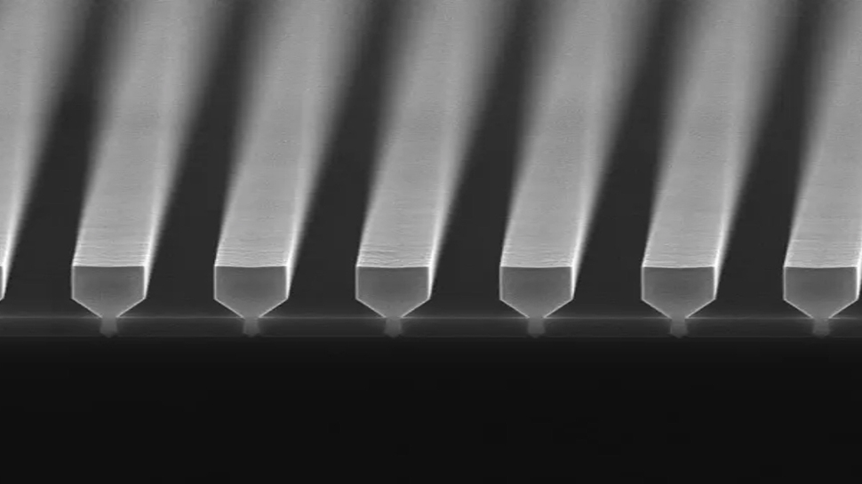
Researchers at Imec have achieved a major breakthrough in the field of silicon photonics by developing a method to grow lasers directly on silicon wafers. This innovation involves using gallium arsenide, a material that doesn’t naturally bond with silicon, which has the potential to lower costs and enhance the performance of photonic chips for applications in AI and telecommunications. By addressing the challenge of efficiently generating light with silicon, this technology could revolutionize data transmission using light instead of electrical signals. The approach, detailed in a Nature paper, leverages nano-ridge engineering to reduce defects and improve laser performance. The lasers, operating at room temperature with low current thresholds and high output powers, emit light at a shorter wavelength than traditional telecommunications lasers. Imec’s pioneering work opens up possibilities for scalable and cost-effective integration of lasers into silicon photonics, laying the foundation for advanced optical devices in the future.


Recent Posts1